


As IFTLE has actually described formerly, Investments in semiconductors will certainly not prosper without financial investments in advanced packaging. The CHIPS for America program, concurring with this facility, has actually introduced that it will certainly sustain the advancement of advanced packaging modern technology in the USA that can be moved to manufacturing centers, consisting of receivers of CHIPS IC manufacturing rewards.
The National Advanced Packaging Manufacturing Program (NAPMP) is a $3 billion federal government program to create important advanced packaging innovations and sustain their change to united state manufacturing entities. (Number 1).
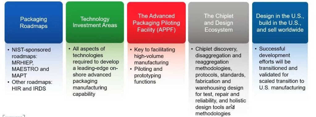
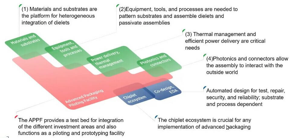
The complete vision for the NAPMP has actually been set out in this white paper.The program will certainly buy the adhering to 6 concern research study locations:
Products and substratums.
Devices, devices, and procedures.
Power distribution and thermal administration for advanced packaging settings up.
Photonics and adapters that interact with the outdoors.
A chiplet ecological community.
Co-design of multi-chiplet systems with automated devices.

As IFTLE has actually shared formerly Subramanian (Subu) S. Iyer signed up with the CHIPS for America’s R&D workplace as the supervisor of the National Advanced Packaging Manufacturing Program (NAPMP). Iyer brings substantial commercial and scholastic experience and competence in microelectronics and packaging.
The NAPMP will certainly develop an advanced packaging piloting center (APPF) (or centers)“…to help accelerate the transfer of innovations in packaging, equipment, and process development into manufacturing” Where everything integrates:
Financial investment locations are anticipated to get in touch with tasks at the APPF. The team might think about prototyping cutting-edge layout concepts from the area.
The APPF is:
Where effective advancement initiatives will certainly be transitioned and verified for scaled change to united state manufacturing.
A vital center for modern technology transfer to high-volume manufacturing.
The APPF might consist of:
Integrated procedure streams that can get to industrial range.
Confirming brand-new modern technology specs, compatibility with various other procedures, return, and dependability.
Examining innovations for scaled change to united state manufacturing.
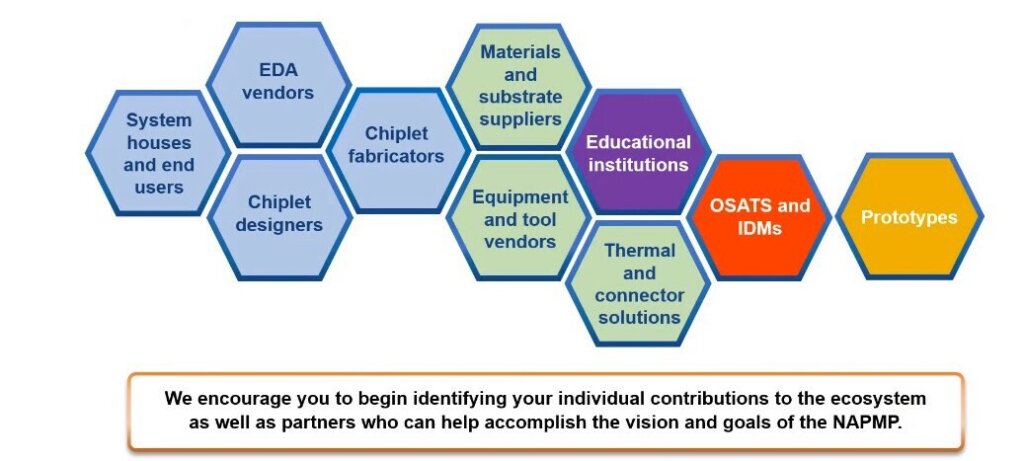
The program will certainly additionally sustain the advancement of electronic devices to decrease the moment and price of advanced packaging design. The NAPMP is hired to function very closely with the National Semiconductor Innovation Facility (NSTC), the semiconductor-related Manufacturing United States Institutes, the CHIPS Assessment Program, and united state sector and academic community.
The NAPMP anticipates to launch its initial financing chance (anticipated to be in the products and substratums location) in very early 2024.
Products and Substrates
According to NAPMP magazines,“The key requirements of new substrates include multiple levels of fine wiring and via pitches, low warpage, large area, and the ability to integrate active and passive components.”
Products and substratums are the system on which advanced packaging is constructed.
These substratums or adjoin textiles (IF) might be based upon silicon, glass, or natural products and can consist of fan-out wafer-level procedures.
The IF demands to.
work with advanced and tradition nodes and various semiconductor product systems.
have integrable energetic and easy elements.
work with either mass reflow, thermal compression bonding, or crossbreed bonding.
Meet ecological and sustainability objectives.
For all the most recent in Advanced Packaging remain connected to IFTLE … … … … … ……


